|
|
|
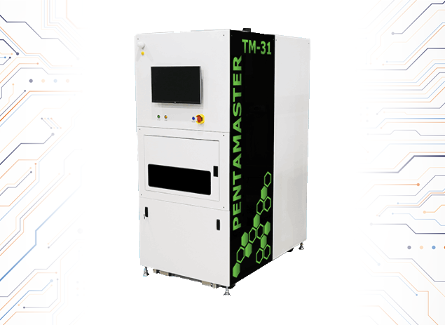
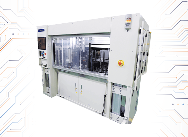
Prober designed for a wafer aiming at Low cost and high throughput |
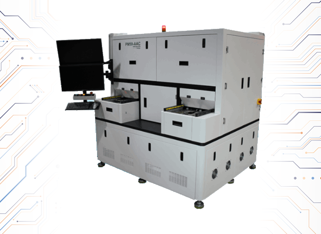
Prober designed to test a double-sided wafer |
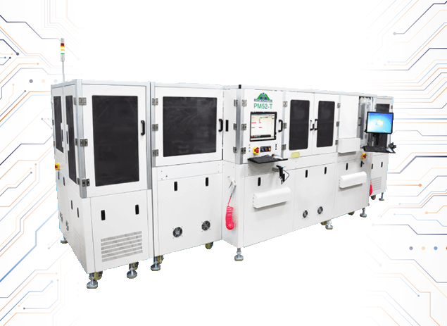
Prober designed aiming to flexibly satisfy the customers' demands |
|
|
XY Compensation (PFC original method) and Profiling compensate the position even if a wafer is expanded by the temperature. |
XY Compensation (PFC original method) and Profiling compensate the position even for a warped wafer. |
XY Compensation (PFC original method) and Profiling compensate the position even if a wafer is expanded by the temperature. |
Record of Alignment success for customers' products is 100%. (In Japan) |
|
|
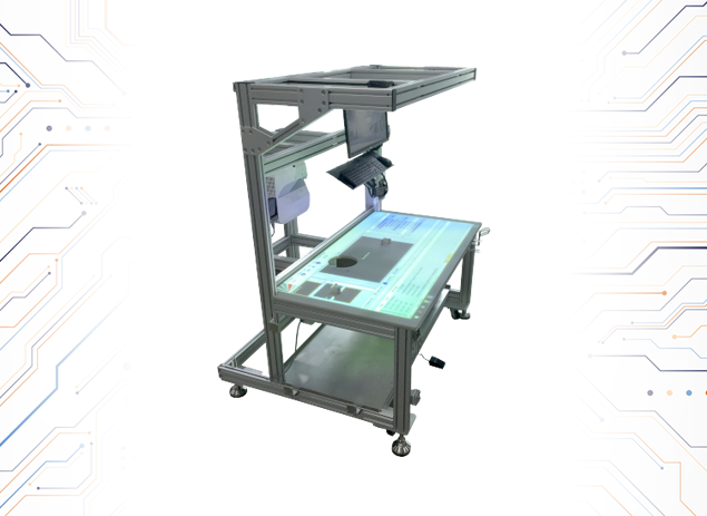
Chip probing is executed by Individual Alignment + Wafer Adaptor . (OP) |
Accurate RDS(on-resistance) is measured by making Kelvin connection at the drain side on the back of wafer and adjusting its drain-sense-position to the source-sense-position. |
Chip probing is executed by Individual Alignment + Wafer Adaptor . (OP) |
Capable of Multi-TEG (more than 2 different kinds on a wafer), etc.
by probing in a chip (Micro Probing). |
|
|
Large diameter Pre-alignment chuck can handle a warped wafer,
thin wafer and TAIKO™ Wafer.(OP) |
Quick Loader can reduce the Load/Unload time per sheet to half. (OP) |
Quick Loader can reduce the Load/Unload time per sheet to half. (OP) |
Quick Loader can reduce the Load/Unload time per sheet to half. (OP) |
|
|
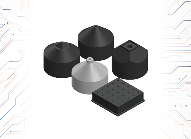
Surface finish for your usage, such as gold plate, nickel plate, etc. |
Large current/High voltage probing is supported by the wafer clamp system with the ceramic blade. |
Surface finish for your usage, such as gold plate, nickel plate, etc. |
Supports the high temperature range 50 ℃ to 150 ℃ and precise thermal control 25℃±0.3℃. (OP) |
|
Supports the high temperature range 50 ℃ to 150 ℃ and precise thermal control 25℃±0.3℃. (OP) |
|
|
Surface of the chuck: More than-80db (*1) |
|
|
High rigidity cabinet made by the iron surface plate and the welding frame |
|
|
Non-magnetic spec is available for a magnetic device. (OP)(*2) |
|
Non-magnetic spec is available for a magnetic device. (OP)(*2) |
|
|
- Low cost, high throughput
- Small space (footprint), power-saving design
- Stable operation (more than MTBF5000 hours)
|
|
|
|
|
100mm (4 inch) to 200mm (8 inch) |
200mm (8 inch)
to
300mm (12 inch) |
|
|
|
|
|
|
Driven by linear motor (Repeat accuracy:1um) |
|
|
Small space: (W) 1200mm × (D) 860mm |
Small space:
(W) 1615mm
×
(D) 1000mm |
|
|
- Total: PCP series more than 430 sets (As of April 2018)
- We can respond to your request flexibly.
- We can offer special price for the purchase of several sets together.
|