
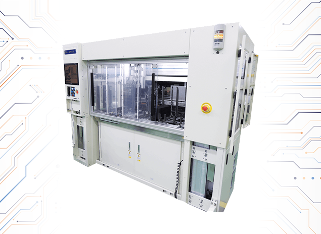
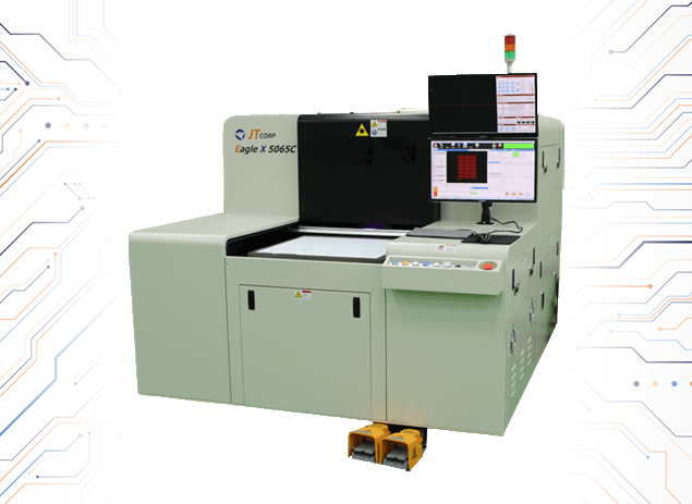
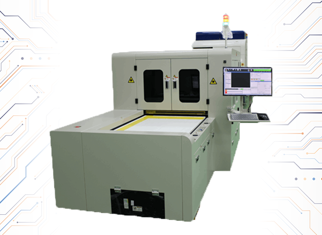
UV Cutting System
Eagle X5065C Laser Cutting System with UV Laser Apply : Pi Film, Coverlay, PCB, FPCB, RF-PCB, SLP, PPG, Cu Plate, Ag Plate, etc. Cutting Application
Our Laser Application Systems for semiconductor manufacturing offer a range of wafer cutting and dicing solutions, including laser-based methods that provide precise and efficient processing. Our systems include the UV Cutting System, Trooper-L Wafer-Level Laser Marking Handler, Laser Repair Application, Laser Direct Patterning System with IR Laser, and CO2 Cutting System. All of these are designed to meet our customers’ needs.
At ![]() 4JMSolutions, we understand the intricate demands of semiconductor manufacturing, and it’s precisely why our advanced Laser Application Systems are tailor-made for the job. From intricate wafer cutting to precise laser dicing, our array of systems ensures not just efficiency but also unparalleled accuracy. The UV Cutting System, for instance, is ideal for a myriad of materials, including Pi Film and RF-PCB, boasting a superior cutting speed and impeccable accuracy.
4JMSolutions, we understand the intricate demands of semiconductor manufacturing, and it’s precisely why our advanced Laser Application Systems are tailor-made for the job. From intricate wafer cutting to precise laser dicing, our array of systems ensures not just efficiency but also unparalleled accuracy. The UV Cutting System, for instance, is ideal for a myriad of materials, including Pi Film and RF-PCB, boasting a superior cutting speed and impeccable accuracy.
On the other hand, the Trooper-L Wafer-Level Laser Marking Handler is a testament to innovation, bringing high precision laser marking on a Solid Granite Platform, ensuring precision and stability in every mark. Our Laser Repair Application – Eagle X7120RE uses the precision of IR wavelength to seamlessly repair and open short parts in ag paste, while the Laser Direct Patterning System with IR Laser – Eagle X7150H excels in fine pitch patterning, catering to diverse materials like Silver Paste and Transparent Electrode.
Lastly, for those seeking optimal laser cutting with a broader wavelength spectrum, our CO2 Cutting System – Eagle X5200G promises to deliver. All these systems embody our commitment to our clients, and at ![]() 4JMSolutions, we don’t just provide machinery; we offer holistic solutions ensuring our customers always have the edge in semiconductor manufacturing.
4JMSolutions, we don’t just provide machinery; we offer holistic solutions ensuring our customers always have the edge in semiconductor manufacturing.
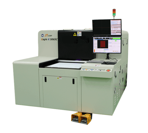
Eagle X5065C Laser Cutting System with UV Laser Apply : Pi Film, Coverlay, PCB, FPCB, RF-PCB, SLP, PPG, Cu Plate, Ag Plate, etc. Cutting Application
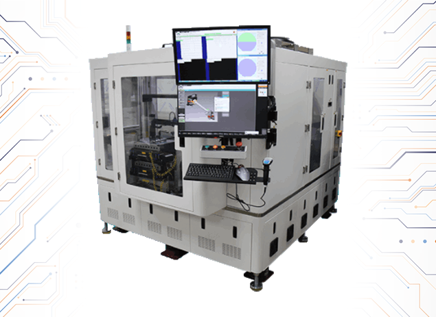
Trooper-L Wafer-Level Laser Marking Handler It is an innovative wafer-level laser marking handler which offers high precision laser marking capable of achieving an accuracy reading
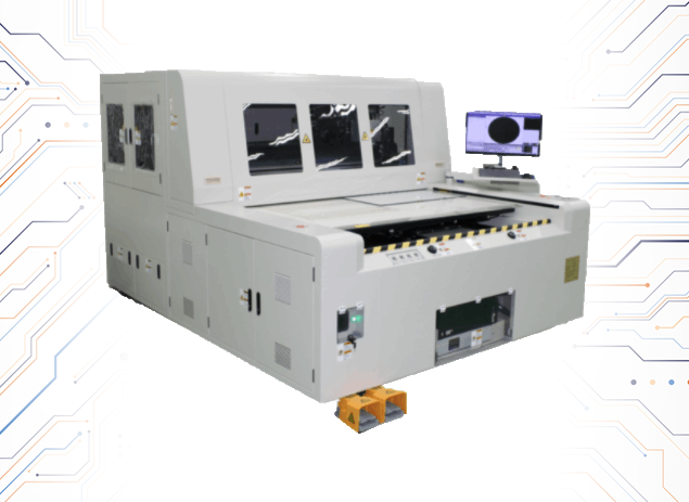
Eagle X7120RE Laser Repair Application Repairing Application by IR Wavelength Equipment to open the short part of each channel in ag paste using laser Beam
Eagle X7150H Laser Direct Patterning System with IR Laser Fine Pitch patterning using Laser and Scan Head Apply : Silver Paste and Transparent Electrode (ITO,
Eagle X5200G Laser Cutting Application Cutting Application by CO2 Wavelength Film Cutting Beam Spot Size Control : Max 100㎛ ~ Max. Cutting Speed : Max
![]() 4JMSolutions (Malta) Ltd. was founded in 2008 on a solid base of international servicing and more than 25 years of high end industrial experience. Based on the solid principal of providing solutions where the equipment offered is a byproduct of the solution.
4JMSolutions (Malta) Ltd. was founded in 2008 on a solid base of international servicing and more than 25 years of high end industrial experience. Based on the solid principal of providing solutions where the equipment offered is a byproduct of the solution.