Home / Equipment / Semiconductor Machines And Manufacturing Equipment / Front-End / Raw Wafer Mapping

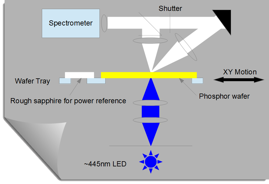
Conventional white LEDs are fabricated from a combination of blue emitting diodes and yellow phosphorescent material.
Some of the blue light is absorbed to make yellow light, and some is transmitted.
A precise ration of blue and yellow is required to make a specific white.
YWafer-YB (yellow and blue) was built on the fundamental design of the YWafer-GS transmission measurement mapping where the broad
band transmission source was replaced with a standard blue LED typically used to make the above type of white light emitting diodes.

In order to properly characterize the phosphor emission and light dispersion, multiple angles of measurement are provided.
(typically 45 or 60 degree from normal).
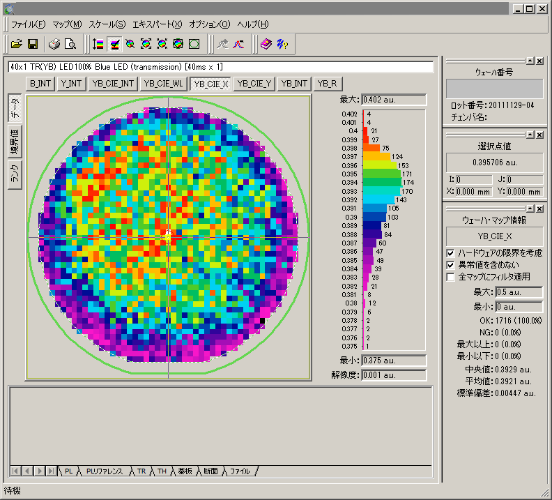
This allows detailed analysis of the color coordinate dispersion across the wafer.

YWafer YB is designed to provide the best reproducibility in wafer to wafer comparison and aims to help phosphor plat
makers attain the uniformity and color target for white LED fabrication.
Both YWafer GS4 and RD8 can be configured for phosphor characterization, but only RD8 can also be configured to measure the phosphor thickness, another important parameter.
![]() 4JMSolutions (Malta) Ltd. was founded in 2008 on a solid base of international servicing and more than 25 years of high end industrial experience. Based on the solid principal of providing solutions where the equipment offered is a byproduct of the solution.
4JMSolutions (Malta) Ltd. was founded in 2008 on a solid base of international servicing and more than 25 years of high end industrial experience. Based on the solid principal of providing solutions where the equipment offered is a byproduct of the solution.