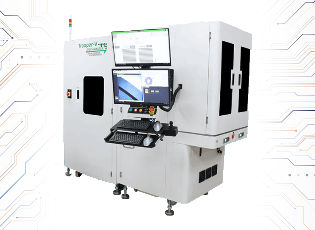
Trooper-V Wafer-Level AOI Handler for Wafer Reconstruction
Trooper-V Wafer-Level AOI Handler for Wafer Reconstructio Trooper-V is a high speed wafer-level AOI handler. It is designed with Rotatable Lens Turret concept which offers
Home / Equipment / Semiconductor Machines And Manufacturing Equipment / Front-End / Wafer Reconstruction
Wafer reconstruction is a pivotal procedure in semiconductor manufacturing. It pertains to the process of rearranging functional chips on sticky tape affixed to a wafer ring post the sawing phase. The essence is to transform standard 12-inch wafers into sizes like 8, 6, 5, or 4 inches, or even reorganize chips based on specific features or grades.
One exemplary wafer reconstruction machine to note is the “Trooper-V,” a high-speed, wafer-level AOI (Automated Optical Inspection) handler. With its groundbreaking Rotatable Lens Turret concept, Trooper-V is adept at catering to varied die sizes and types. Its diverse magnification levels, ranging from 2.0x to 7.0x, ensure unparalleled precision in wafer inspection. Notably, Trooper-V has an impressive efficiency rate, requiring a mere 2 minutes for the scrutiny of an entire wafer that may contain around 70,000 dies.
Some of its standout features include:
Wafer reconstruction machines, epitomized by the Trooper-V, are essential tools in the semiconductor landscape, ensuring that each wafer undergoes rigorous quality checks before being deemed fit for use.

Trooper-V Wafer-Level AOI Handler for Wafer Reconstructio Trooper-V is a high speed wafer-level AOI handler. It is designed with Rotatable Lens Turret concept which offers
The Vanguard of Flip Chip Bonding Technology The transformative wave of miniaturization and enhanced connectivity in the semiconductor world is largely driven by pioneering technologies
4JMSolutions – Pioneering Excellence with Advanced Die Bonder Machines Die bonding, often regarded as the heartbeat of the semiconductor assembly process, finds its true innovation
Die Sorter Machines 4JMSolutions takes pride in its lineup of state-of-the-art Die Sorter Machines, which come fully integrated with AOI (Automated Optical Inspection) systems. Die
4JMSolutions is proud to offer advanced wafer Automatic Optical Inspection (AOI) systems from leading manufacturers. These systems play a crucial role in the semiconductor manufacturing
The Trooper-BI Wafer-Level VCSEL/LED/Micro LED Burn-in wafer level testing system is highly versatile and can accommodate a wide range of units, up to 7,200 at
Our Laser Application Systems for semiconductor manufacturing offer a range of wafer cutting and dicing solutions, including laser-based methods that provide precise and efficient processing.
![]() 4JMSolutions (Malta) Ltd. was founded in 2008 on a solid base of international servicing and more than 25 years of high end industrial experience. Based on the solid principal of providing solutions where the equipment offered is a byproduct of the solution.
4JMSolutions (Malta) Ltd. was founded in 2008 on a solid base of international servicing and more than 25 years of high end industrial experience. Based on the solid principal of providing solutions where the equipment offered is a byproduct of the solution.