

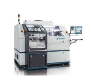
FC-1250 Chip to Substrate or Leadframe
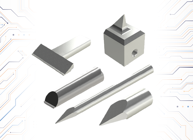
FC-1250 Chip to Substrate or Leadframe SUPH up to 15,000 Die size 0.3x8mm BH Force 0.5-10N Accuracy ±10µm Face-down; Dipping Request More Information Related Die
Die bonding, often regarded as the heartbeat of the semiconductor assembly process, finds its true innovation in the technologically superior machines provided by ![]() 4JMSolutions. This crucial die attach process, which involves affixing a die/chip to a substrate or leadframe, is central to semiconductor fabrication. With the relentless pace of miniaturization and the ever-growing need for precision, choosing the right die bonder machine becomes paramount.
4JMSolutions. This crucial die attach process, which involves affixing a die/chip to a substrate or leadframe, is central to semiconductor fabrication. With the relentless pace of miniaturization and the ever-growing need for precision, choosing the right die bonder machine becomes paramount.
Introducing 4JMSolutions’ premier die bonder machines:
Redefining accuracy and efficiency, the FC-1210 is built to handle a wide range of die sizes from 0.5-6mm, with an extended option for 6-20mm. Boasting an impressive SUPH (Sorted Units Per Hour) of up to 5,500, its precision is undeniable with a local accuracy of ±3µm and a global accuracy of ±5µm. What sets this machine apart is the inclusion of a bond force sensor, ensuring optimal force application during the die bonding semiconductor process.
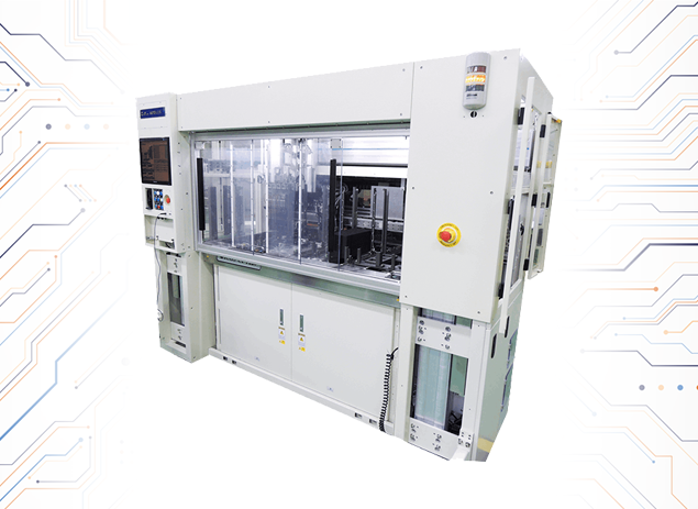
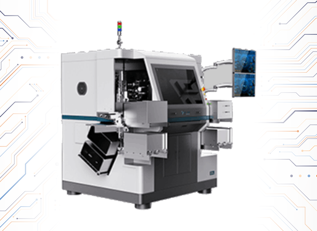
A true titan in the die bonder lineup, the FC-1250 is engineered for high-speed operations with a staggering SUPH of up to 15,000. Catering to die sizes of 0.3x8mm, this machine encapsulates versatility and precision. It integrates a BH Force range of 0.5-10N, ensuring gentle yet firm bonding. The machine’s accuracy stands at ±10µm, and it offers diverse bonding techniques: face-down dipping and a combination of face-up/face-down with BH/Chunk table heating and dipping.
FC-1250 Chip to Substrate or Leadframe SUPH up to 15,000 Die size 0.3x8mm BH Force 0.5-10N Accuracy ±10µm Face-down; Dipping Request More Information Related Die
FC-1210 Chip to Substrate or Leadframe SUPH up to 5,500 Die Size 0.5-6mm (6-20mm option) Bond Force Sensor Accuracy ±3µm local ±5µm global Face-up/Face-down; BH/Chunk
![]() 4JMSolutions (Malta) Ltd. was founded in 2008 on a solid base of international servicing and more than 25 years of high end industrial experience. Based on the solid principal of providing solutions where the equipment offered is a byproduct of the solution.
4JMSolutions (Malta) Ltd. was founded in 2008 on a solid base of international servicing and more than 25 years of high end industrial experience. Based on the solid principal of providing solutions where the equipment offered is a byproduct of the solution.